Hype or no, Nanotechnology is here to stay, Prof. Chacko Jacob explained at the recently held Science Communication Conclave at IIT Kharagpur
An innocuous looking pouch. But as you open it and place it on top of your knee that has been bothering you no end, a warmth emanates and spreads to your aching joint. This is ‘Heat Pax’, the “Air activated body warmer”, as the label says. [1]
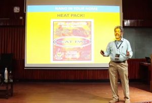 Inside though, a marvellous chemistry is at work. The airtight wrapper of this pack contains fine iron particles combined with vermiculite (a form of clay which holds water) and carbon or charcoal. When the wrapper is torn and the contents are exposed to air, the iron, highly reactive in its ground form, reacts with the air exothermically, producing oxide a la rust, and heat. The charcoal disperses the heat.
“Someone has just commercialized rusting,” guffawed Prof. Chacko Jacob while handing out packets of ‘Heat Pax’ for all to see. Speaking on ‘Nanotechnology: Hype, hope or reality’ at the recently held Science Communication Conclave (Feb 28-29) at IIT Kharagpur, Prof. Jacob was explaining to his audience the science of the small that makes such amazing chemistry possible. With the Materials Science Centre of IIT Kharagpur for close to two decades, Prof. Jacob specializes in making nano structures through the chemical vapour deposition (CVD) technique.
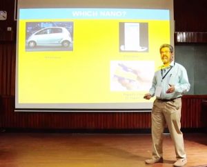
 We invariably associate ‘nano’ with everything small – Tata Nano, iPod Nano, or even the Paper Pro Nano desk stapler. But, Prof. Jacob explained, “In the world of science, ‘Nano’ does not necessarily mean small. What I want you to recognize is that in the world of nanotechnology something is happening that makes the same material behave very differently when it is small than when it is at the conventional scale.”
Example? A cluster of 48 molecules of ice melts at 93 Kelvin or minus 180 degree centigrade. [2] Minuscule particles of gold, iron and nickel melt at a far lower temperature than their normal melting points. Their colour changes too when they are tiny, as do their electrical properties. Prof. Jacob said, “In working with nanomaterials, I am working not with something just really small, but something that is very, very different in behaviour from the bigger pieces of the same material that I am familiar with.”
 People down the ages have been aware of what can be called the marvel of the tiny, although they could not put a name to it. Take the stained glass windows in the cathedrals all over Europe that go back to the 12th century or even earlier. “They put metallic salts in the glass during processing to get color, although they did not know they were using ‘nanotechnology’. By controlling how these metal containing glasses were heated up, one could decide the colour since the color depended on the shape and size of the metal nanoparticles that were formed,” said Prof. Jacob. [3]
Silver halide photography of the early 20th century also used nanotechnology as silver nanoparticles helped capture the image. [4] Even now, as lenses are coated with anti-reflective material that are nothing but “very, very thin films in the order of tens or hundreds of nanometres”, we are using nanotechnology.
 It was the advance of microscopy that made it possible to see at the atomic and molecular level that gave a fillip to nanotechnology. “It is because we can see at this level, and can manipulate objects the way we want, that we can move at a much faster pace,” said Prof. Jacob.
A casual search of the use of nanotechnology in today’s world revealed innumerable applications of nanotechnology in modern life. Take the use of embedded nanoparticles to create stain-repellent khakis, Toyota’s use of nanocomposites in a bumper that make it 60% lighter and twice as resistant to denting and scratching, Wilson’s (a sporting brand) use of a nanocomposite coating on tennis balls that keeps them bouncing twice as long as an old-style ball, the use of nanoparticles in sunscreens that make them extremely effective at absorbing light, especially in the ultra-violet (UV) range, the use of nanoparticles to make synthetic bone, the use of fluorescent nanocrystals as fluorescent markers in biology and drug-conjugated nanocrystals that attach to proteins and enable the filming of protein trafficking.
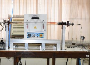
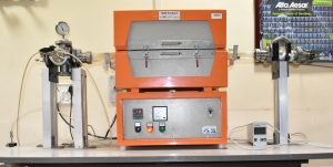
In his own lab at the Materials Science Centre, Prof. Jacob makes nanostructures of various dimensions with various materials such as carbon, silicon carbide, tungsten oxide, copper oxide, zinc oxide etc. Through the CVD process, nanomaterials are produced, either in the form of films or wires,, or even hollow structures.
Prof. Jacob says, “We have worked on silicon carbide, which can be grown as nanorods and nanowires. When they are coated with an alloy of gold-palladium nanoparticles, they tend to show superhydrophobic behaviour or self-cleaning behaviour.” The team is trying to tune the adhesion state of a liquid droplet on the superhydrophobic surfaces by electrowetting so that the property can be exploited for various applications in microfluidics, lab on chip and biotechnology.
The group has started CVD synthesis of a new class of materials called transition metal dichalcogenides (TMDCs) which include molybdenum disulphide – a two dimensional material, which, Prof. Jacob, says, is regarded as an “after-graphene kind of material.”
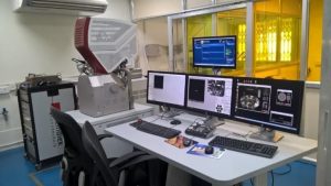
At the Micro and Nano Robotics and Fabrication Facility, a facility created by the Institute and involving eight faculty members and their research groups from various departments at present, the group works with the Dual Beam Tescan Lyra 3, which is “basically an electron microscope with an added ion beam of gallium with which we can fabricate, cut nano structures, join them together, make measurements — a little nano tool box really,” explains Prof. Jacob. They also work with a 3D printer, Nanoscribe, which is able to print very small structures with a very high resolution inside a light sensitive polymer with a laser using a process called two photon polymerization. This has applications in micro-nano fluidics, sensors, photonics, scaffolds for cell growth, etc.
So where is nanotechnology headed? “Towards the manufacture of more evolved sensors, supercapacitors, micro and nanofluidics, drug delivery, nano robotics, opto-electronics, nano electronics, nano composites, self-cleaning coatings,” answers Prof. Jacob.
Nanotechnology has gone through what he believes is the “hype cycle”. [5] The peak in publicity and public interest in Nanotechnology that followed Richard Feynman’s 1959 talk [6] on miniaturization (“There’s plenty of room at the bottom”) at the annual American Physical Society meeting at Caltech), has petered out and settled into a plateau as more and more of nanotechnology becomes part of everyday life. Prof. Jacob explains, “This is the ‘plateau of Productivity’ when mainstream adoption starts to take off as it becomes evident that the technology’s broad market applicability and relevance are clearly paying off.” So hype or no, nanotechnology is here to stay.
References:
[1] https://www.heatpax.com/
[2] https://doi.org/10.1103/PhysRevLett.103.073401
[3] http://nano–tech.blogspot.com/p/history.html
[4] https://www.iinano.org/19th-century
[5] https://www.gartner.com/en/research/methodologies/gartner-hype-cycl
[6] https://ieeexplore.ieee.org/document/128057/